-
KOSPI 2812.05 +41.21 +1.49%
-
KOSDAQ 756.23 +6.02 +0.80%
-
KOSPI200 376.54 +6.64 +1.80%
-
USD/KRW 1373 3.00 -0.22%
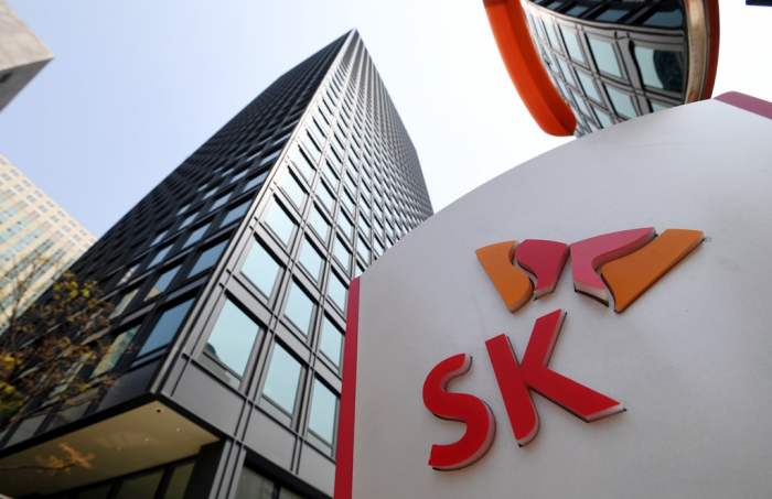
SK to build first chip packaging plant in US with $22 bn investment
Corporate investment
SK to build first chip packaging plant in US with $22 bn investment
Most of the new spending is earmarked for chips, green energy and biotech sectors, while SK Hynix posted record Q2 sales
By
Jul 27, 2022 (Gmt+09:00)
4
Min read
News+
Related Article
The Korea Economic Daily App


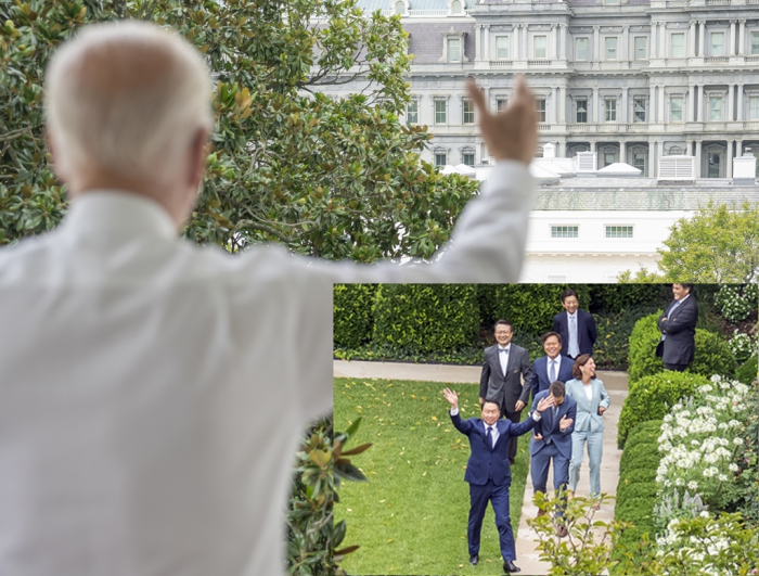
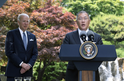
WASHINGTON DC – SK Group, South Korea’s second-largest conglomerate, said on Wednesday it will build its first memory chip packaging facility in the US as part of a fresh $22 billion investment in the US manufacturing sector.
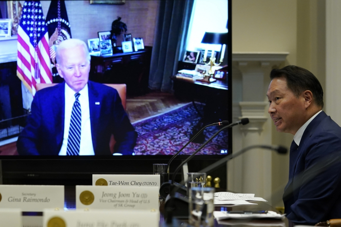
The announcement came during a videoconference meeting between visiting SK Chairman Chey Tae-won and US President Joe Biden at the White House to discuss SK’s investments in various US business sectors, particularly in semiconductor technology.
The new spending plan comes on top of SK’s $7 billion investment, announced earlier, to build two electric vehicle battery plants in Tennessee and Kentucky as part of a joint venture with Ford Motor Co.
The US president, who is recovering from COVID-19, participated virtually in the meeting, while US Commerce Secretary Gina Raimondo and other White House officials joined Chey in person.
Addressing Chey by his English name Tony during the online meeting, President Biden welcomed the announcement, calling it one of the most "significant investments" ever seen in the US.
The investment, Biden said, showed that the "United States, Korea and its allies are back and winning the technology competition of the 21st century.”
SK Group said in a statement that its investment, to be made in semiconductors, green energy and bioscience, will create “tens of thousands of new high-tech, high-paying American jobs."
The virtual meeting comes as the Biden administration seeks the cooperation of its Asian allies, including Korea, to reinforce the US-led supply chain of critical components such as semiconductors.
CHIP INVESTMENT TAKES THE LION’S SHARE
Of the $22 billion in new US investment, SK Group said about 70%, or $15 billion, will go toward the semiconductor business.
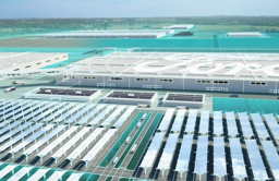
More specifically, the Korean conglomerate will select a US university to jointly conduct semiconductor research and development (R&D) projects. SK said it will also establish an advanced memory chip packaging facility in the US.
SK didn’t provide details such as the location and timing of the construction of its first chip packaging plant in the US.
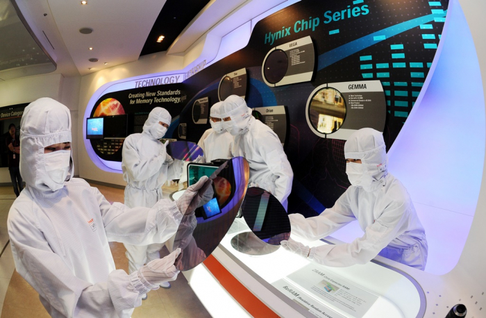
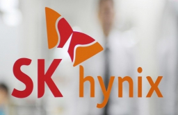
SK Hynix Inc., the world’s second-largest memory chipmaker, earlier said it will spend more than 1 trillion won ($762 million) to build an open-ended R&D center somewhere in the western US.
SK Hynix currently operates a chip packaging factory in Chongqing, China.
SK Group said on Wednesday it will invest $5 billion in the US green energy sector, including the smaller nuclear reactor business, and $2 billion in the cell and gene therapy sectors and other biotechnology businesses.
The US investment plan followed SK’s announcement in May that the group will invest 247 trillion won globally in key growth sectors such as semiconductors, batteries and biotechnology over the next five years.
SK said at the time that 142.2 trillion won, or nearly 60% of total spending through 2026, is earmarked to set up a local semiconductor ecosystem, which included the launch of a chip cluster, expansion of chip fabrication facilities and increased buying of chipmaking equipment. About 179 trillion won, or 73% of its total investment plan, is set aside for spending in Korea, it said.
BIDEN’S SEOUL TRIP
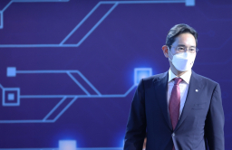
In May, the US president visited Seoul as part of his Asia trip, meeting with the leaders of large Korean companies, including Samsung Group Vice Chairman Jay Y. Lee and Hyundai Motor Group Chairman Chung Euisun.
During Biden’s stay in Seoul, both Samsung and Hyundai Motor announced multi-billion-dollar spending plans to expand production plants in the US, prompting speculation that SK would follow suit.
Hyundai Motor Co. said in May it will spend $10.5 billion on the US auto industry through 2025 as it aims to expand its future mobility business in the world’s second-largest car market.
Samsung showcased its advanced chipmaking technology to the visiting US president at the company’s semiconductor plant in Pyeongtaek, near Seoul.
Samsung announced in late May that it will spend 450 trillion won globally over the next five years in strategic sectors such as semiconductors, biotechnology and 6G telecommunications.
HYNIX POSTS RECORD Q2 SALES, OUTLOOK DIM
On Wednesday, SK Hynix posted record second-quarter sales and strong operating profit, buoyed by robust sales of NAND flash chips and positive currency effects.
Operating profit in the April-June period rose 55.6% from a year ago to 4.19 trillion won, the highest since 2018.
Its second-quarter sales increased 33.8% on year to an all-time high of 13.81 trillion won.
The company warned, however, that semiconductor demand will likely dip in the second half, especially for chips used in personal computers and smartphones.
Company executives said its DRAM and NAND flash inventory levels have already gone up by around one week, reflecting weakening demand.
Last week, the chipmaker said it is delaying a 4.3 trillion won plan to build a new NAND chip factory amid growing global uncertainty and falling chip prices.
Earlier, SK Hynix had said it plans to expand capacity with a new NAND plant, dubbed M17, in Cheongju, North Chungcheong Province, 140 km south of Seoul, with construction set to begin next year and continue through 2025.
But the company said on Wednesday it plans to add four new production lines at a chip cluster in Yongin, 40 km south of Seoul, as scheduled.
Write to Kyung-Min Kang and In-Seol Jeong at Kkm1026@hankyung.com
In-Soo Nam edited this article.
More To Read
-
 Korean chipmakersSK Hynix puts $3.3 billion factory plan on hold amid global uncertainty
Jul 20, 2022 (Gmt+09:00)
-
Jul 14, 2022 (Gmt+09:00)
-
 Corporate investmentHyundai Motor to launch investment affiliate in US for further growth
Jul 01, 2022 (Gmt+09:00)
-
 Corporate investmentSamsung to invest $355 billion in chip, biotech, 6G over five years
May 24, 2022 (Gmt+09:00)
-
 Corporate investmentSK takes aim at chips, batteries, bio with $195 billion investment
May 26, 2022 (Gmt+09:00)