-
KOSPI 2812.05 +41.21 +1.49%
-
KOSDAQ 756.23 +6.02 +0.80%
-
KOSPI200 376.54 +6.64 +1.80%
-
USD/KRW 1373 3.00 -0.22%
Samsung to invest $15 bn in semiconductor R&D complex
Korean chipmakers
Samsung to invest $15 bn in semiconductor R&D complex
The Korean tech giant aims to narrow the gap with TSMC and address competition from smaller rivals with technology development
By
Aug 19, 2022 (Gmt+09:00)
5
Min read
News+
Related Article
The Korea Economic Daily App


Samsung Electronics Co., the world’s top memory chipmaker, plans to spend 20 trillion won ($15.1 billion) by 2028 on an advanced semiconductor research and development complex to secure a competitive edge in an intensifying battle against rivals such as Taiwan Semiconductor Manufacturing Co. (TSMC).
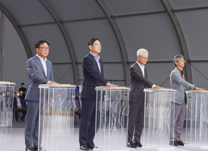
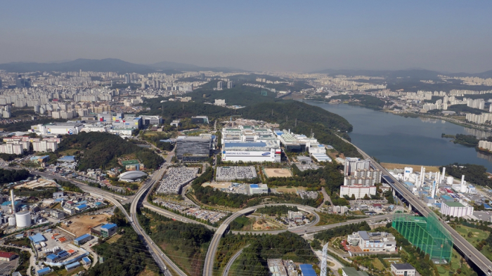
Samsung on Friday broke ground for the complex in Giheung, Yongin, about 50 kilometers south of Seoul, earmarked for key R&D in its memory, fabless system semiconductors, foundry and other sectors. The company is poised to operate a dedicated production line for the R&D center from 2025.
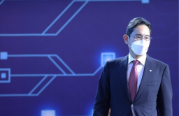
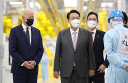
“We begin a new challenge on the Giheung campus where the first shovel hit the ground 40 years ago to build a semiconductor factory,” Samsung Vice Chairman Jay Y. Lee said in the groundbreaking ceremony with the slogan “We create the future with technology that does not exist in the world.”
“We need super excellent technology that can lead the global market without being hit by a crisis,” Lee stressed in his first public appearance since he has had his right to work restored.
The tech giant 1983 began its semiconductor business in Giheung and the campus made key achievements such as the world’s first development of the 64Mb DRAM in 1992.
When Lee Byung-chul, the late Samsung Group founder and chairman, declared the start of the semiconductor business in that year, Intel Corp. called the current vice chairman’s grandfather a megalomaniac. Japan’s Mitsubishi Research Institute Inc. also issued a report stating five reasons why Samsung would fail in the business.
Samsung, however, stands as the global leader in the memory chip business, defying such disdain, through continuous investments in semiconductor technologies.
TOUGH ENVIRONMENT
But the company’s business conditions have been deteriorating. The US government proposed to form a four-country chip alliance with South Korea, Japan and Taiwan in a move to isolate China from the global semiconductor ecosystem. Participation will definitely prompt China, Samsung’s key customer, to take retaliatory action.
The market share gap with TSMC remains wide in the foundry industry, while Samsung’s smaller rivals are rapidly chasing the frontrunner in the memory chip business.
TSMC has been taking up more than 50% of the global foundry market, while Samsung’s market share has been stagnant at around 18% since 2019.
Smaller rivals are trying to expand their presence. US Micron Technology Inc. last month announced mass production of the world’s first 232-layer NAND chip, while China's Yangtze Memory Technologies (YMTC) said it has delivered samples of its in-house developed 192-layer 3D NAND flash memory to a few customers.
Vice Chairman Lee decided to develop technologies to overcome those issues.
“The US and China cannot directly put pressure on Samsung because it has technology and production capabilities,” said an industry source. “Samsung has no choice but to maintain its technological leadership.”
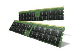
Cutting-edge technologies helped Samsung control global markets. Samsung kept the throne in the memory chip sector with the DDR5 DRAM, which has doubled the performance compared to the DDR4. The prices of DDR5 products were immune to the recent drops in the overall DRAM prices as the models were suitable for artificial intelligence and machine learning, drawing strong demand. Samsung currently led the DDR5 DRAM market.
South Korea, the home to Samsung and the world’s No. 2 memory chipmaker SK Hynix Inc., has been relatively passive in semiconductor technology investments.
Samsung last year spent $6.5 billion on R&D for the semiconductor business, less than half of the $15.2 billion of Intel Corp., according to the industry research firm IC Insights.
The South Korean tech behemoth aims to quickly catch up with TSMC, the global foundry leader with the investment in the R&D complex. Samsung was known to narrow the gap with the Taiwanese maker in the sector for below 10-nanometer process nodes. Samsung’s technologies on the 3-nm process node, the industry’s narrowest circuitry, are superior to those of TSMC.
Samsung plans to manufacture products below 3 nm sooner, improving its competitiveness.
SAMSUNG TO HELP KOREAN SEMICONDUCTOR SECTOR LEAP
Samsung, the country’s largest company by market capitalization, aims to build the new R&D complex as a state-of-the-art facility for future semiconductor technologies.
The planned exclusive fab for the R&D center in the complex is expected to shorten the development period and improve product quality, industry sources said.
“The dedicated production line to the R&D with cutting-edge equipment will allow researchers to conduct various experiments more freely and actively,” said one of the sources.
The R&D complex is expected to help the local semiconductor industry’s ecosystem leap to the next level as it provides a wide range of foundations for delicate and comprehensive research that cover the technologies of each sector.
The semiconductor industry needs systematic and collaborative developments in each field including design, materials, equipment, components, process and inspection. The industry is not a business that can sustain growth with the development of only certain sectors.
“As the semiconductor technology’s ultra-miniaturization into nano units reached physical limitations, their development has slowed down,” said another industry source. “We need a research base that allows experimental and challenging attempts in order to overcome technical difficulties.”
The industry hopes the R&D complex to produce innovative technologies that help not only Samsung but the country’s entire semiconductor ecosystem to evolve.
Write to Shin-Young Park and Ji-Eun Jeong at nyusos@hankyung.com
Jongwoo Cheon edited this article.
More To Read
-
Aug 12, 2022 (Gmt+09:00)
-
 Korean chipmakersS.Korea edges closer to joining US-led chip alliance
Aug 02, 2022 (Gmt+09:00)
-
 Korean chipmakersSamsung's 3 nm chip narrows microchip gap with TSMC
Jun 30, 2022 (Gmt+09:00)
-
May 03, 2022 (Gmt+09:00)
-
 Korean chipmakersSamsung widens lead over rivals with industry’s first advanced DDR5
Mar 26, 2021 (Gmt+09:00)