-
KOSPI 2698.97 +1.30 +0.05%
-
KOSDAQ 740.29 +5.94 +0.81%
-
KOSPI200 359.69 +0.07 +0.02%
-
USD/KRW 1375 6.00 -0.44%
Samsung Electronics to aid foundry clients with state-of-the-art tech
Korean chipmakers
Samsung Electronics to aid foundry clients with state-of-the-art tech
The chipmaker has been bolstering its partnerships with its customers to take on archrival TSMC
By
Jul 05, 2023 (Gmt+09:00)
3
Min read
News+
Related Article
The Korea Economic Daily App


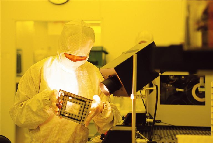
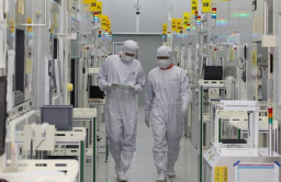
Samsung Electronics Co., the world’s largest memory chipmaker, will provide its foundry clients with state-of-the-art technology to support their businesses and create a stronger contract chipmaking ecosystem.
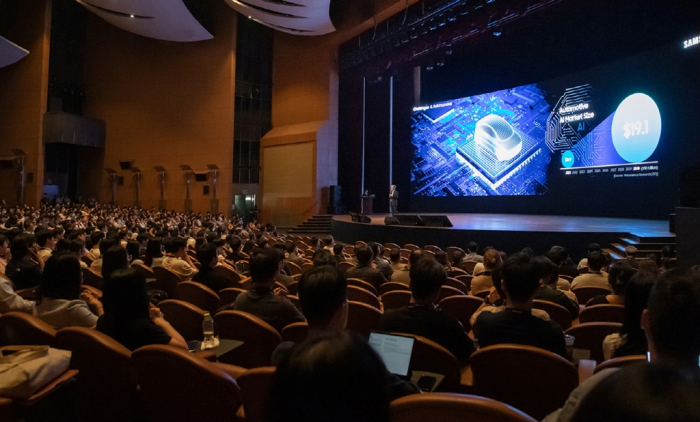
At the Samsung Foundry Forum (SSF) and Samsung Advanced Foundry Ecosystem (SAFE) Forum 2023 held in Seoul Tuesday, the South Korean tech giant unveiled custom-tailored client support programs.
One of those programs is to provide clients with its latest process design kits to assist them in chip design and inspection, which utilize Samsung’s 2- to 3-nanometer chip process technology.
Samsung said it will provide its clients with the kits from the second half of this year.
It also plans to expand its Multi-Project Wafer service, which helps fabless customers produce various prototypes of chip products on a single wafer to cut costs.
Samsung said it will expand the service by more than 10% next year compared to this year.
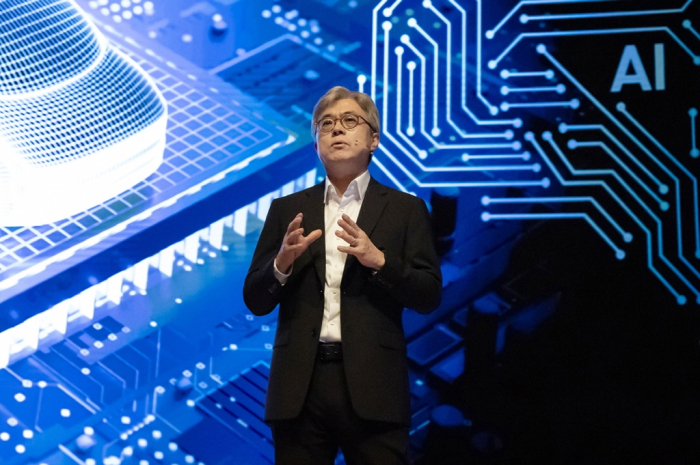
“We will enhance collaboration with our customers and build a stronger chip ecosystem to better respond to the changing semiconductor industry,” said Choi Si-young, Samsung’s foundry business chief, at the annual forum.
MINOR PLAYER IN SYSTEM CHIP ARENA
Samsung Foundry, the Korean company’s contract chipmaking business, has been bolstering partnerships with its clients to enhance its presence in the foundry segment.
Although it is the world leader in the memory sector, which makes DRAM and NAND chips, the company is a distant second in the foundry business with a low double-digit market share after Taiwan Semiconductor Manufacturing Co. (TSMC), which controls more than half of the global market
In the lucrative system chip segment, Korean chipmakers, including Samsung and crosstown rival SK Hynix Inc., take up a mere 3% market share.
To create a mutually beneficial chip ecosystem, Samsung is leading Korea’s efforts to build the world’s largest semiconductor cluster near Seoul by attracting 340 trillion won ($261 billion) in private investment.
Samsung said it will invest around 300 trillion won over the next two decades through 2042 to create the mega chip cluster in Yongin, Gyeonggi Province.
The company said it is also seeking to expand its chip design intellectual property (IP) partnerships with its clients.
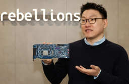
LX SEMICON, REBELLIONS
This year’s Samsung forum drew over 1,100 guests from its foundry partners, some of which showcased their latest technologies.
Ko Dae-hyup, head of research at LX Semicon Co., a leading Korean chip design firm, said the company will expand cooperation with Samsung to advance its display driver integrated circuit (DDIC) chips.
Industry sources said earlier this week LX will ask Samsung to manufacture its latest DDIC chips with advanced chip process machines.
Park Sung-hyun, chief executive of Rebellions Inc., a three-year-old Korean AI chip design startup, said at the forum that its AI chip, ATOM, boasts faster processing speed than its rivals thanks to Samsung’s 5 nm foundry chip manufacturing tech.
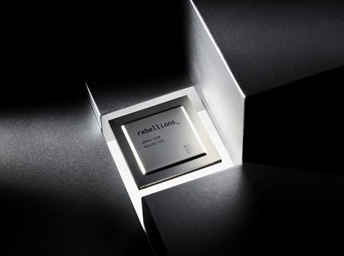
ATOM’s processing speed was up to 3.4 times faster than the same class chips by Qualcomm and Nvidia, according to an industry performance test.
Samsung’s Choi said at the SFF in San Jose, California last month that the company will begin mass production of the 2 nm process for mobile applications in 2025 before expanding to other uses in later years.
Looking ahead, Samsung also confirmed its plans to begin mass production of more advanced 1.4 nm chips by 2027.
Write to Ik-Hwan Kim and Ye-Rin Choi at lovepen@hankyung.com
In-Soo Nam edited this article.
More To Read
-
 Korean chipmakersSamsung’s foundry business to make DDIC chips for LX Semicon
Jul 03, 2023 (Gmt+09:00)
-
 Korean chipmakersSamsung on smooth track to 1.4 nm foundry tech to take on TSMC
Jun 28, 2023 (Gmt+09:00)
-
 Korean chipmakersIntel’s foundry revamp sets off alarm bells for Samsung, TSMC
Jun 22, 2023 (Gmt+09:00)
-
 Korean startupsRebellions CEO aims to outrival Qualcomm within a decade
Apr 10, 2023 (Gmt+09:00)
-
 Business & PoliticsSouth Korea eyes $261 billion chip cluster; Samsung takes lead
Mar 15, 2023 (Gmt+09:00)
-
 Korean chipmakersSystem on chips: Samsung’s new high-stakes foundry business
Mar 09, 2023 (Gmt+09:00)