-
KOSPI 2577.27 -2.21 -0.09%
-
KOSDAQ 722.52 -7.07 -0.97%
-
KOSPI200 341.49 +0.02 +0.01%
-
USD/KRW 1396 -2.00 0.14%
Samsung to produce 290-layer V9 NAND to win chip stacking war
Korean chipmakers
Samsung to produce 290-layer V9 NAND to win chip stacking war
Already the world's top NAND player, Samsung plans to widen its lead by launching 430-layer products next year
By
Apr 11, 2024 (Gmt+09:00)
3
Min read
News+
Related Article
The Korea Economic Daily App


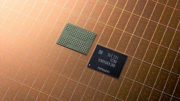
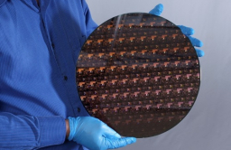
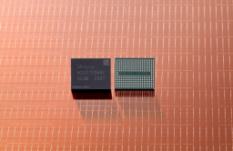
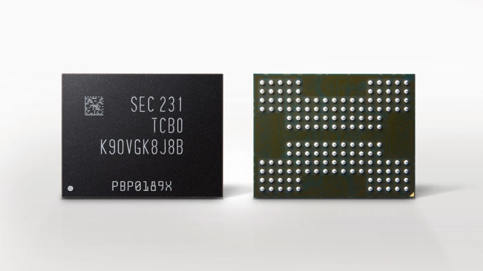
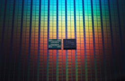
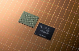
Samsung Electronics Co., the world’s largest memory chipmaker, is set to begin mass production of 290-layer ninth-generation vertical (V9) NAND chips later this month to lead rivals in the industry’s transition to high-stacking high-density flash memory.
The South Korean chipmaker also plans to unveil 430-layer NAND chips next year as demand for high-performance and large storage devices grows in the artificial intelligence era, industry sources said on Thursday.
The V9 NAND is a cutting-edge product that succeeds Samsung’s current flagship 236-layer V8 flash products, targeting large-scale enterprise servers and AI and cloud devices.
What’s significant with the V9 NAND is that Samsung utilizes its double-stack technology, sources said.
Due to technical limitations, triple-stack or triple-level cell technology is widely regarded as the most common method to manufacture around 300-layered chips.
According to market research firm TechInsights Inc., Samsung is expected to unveil a 430-layer 10th-generation NAND chip in the second half of next year.
Sources said that Samsung is expected to use triple-stack technology to make the V10 NAND flash memory.
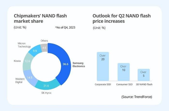
Samsung has been the NAND market leader since 2002.
STACKING TECH WAR INTENSIFIES
Major chipmakers are engaged in a game of chicken in a race to develop advanced chip stacking technology to cut costs and improve performance.
Competition for NAND-based storage devices is fierce as AI chips focus on inference, which requires large-capacity storage devices to store and process images and videos.
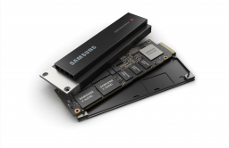
A NAND flash is a type of non-volatile memory chip that stores data even when the power is off. It is used in devices like smartphones, USB drives and servers.
Higher-density NAND chips will accelerate data-intensive environments and workloads such as AI engines and big data analytics. For 5G smartphones, the enhanced capacity can enable faster launching and switching across multiple apps, creating a more responsive mobile experience and faster multitasking.
According to market research firm Omdia, the NAND flash market is expected to grow 38.1% this year after falling 37.7% in 2023.
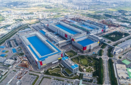
To gain ground in the fast-growing market, Samsung has vowed to invest heavily in the NAND business.
Samsung executives said the company aims to develop over 1,000-layer NAND chips by 2030 for higher density and storage capabilities.
SK HYNIX, YMTC
Samsung’s rivals are also unveiling high-density NAND chips.
SK Hynix Inc., the world’s second-largest memory chipmaker, plans to start producing 321-layer NAND products using its triple-stack technology early next year.
Last August, the company showcased a sample of the 321-layer four-dimensional (4D) NAND at the Flash Memory Summit in Santa Clara, California. SK Hynix said it would start mass production of the 1-terabit (Tb) triple-level cell (TLC) 4D NAND flash in the first half of 2025.
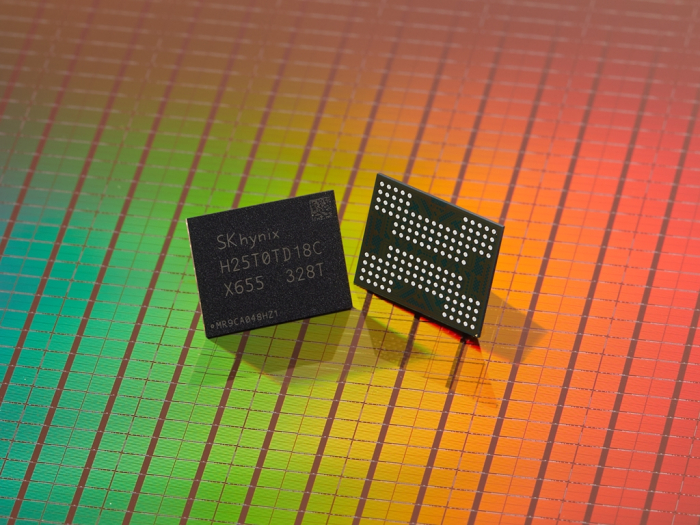
The company said the 321-layer NAND has improved productivity by 59% compared with its 238-layer, 512 Gb 4D NAND chips.
China's Yangtze Memory Technologies Corp. (YMTC), a flash memory specialist, began mass production of a 232-layer NAND product last year and plans to unveil 300-layer chips later this year.
With the growing demand for NAND chips, Samsung’s NAND business swung to an operating profit in the first quarter.
Write to Jeong-Soo Hwang at hjs@hankyung.com
In-Soo Nam edited this article.
More To Read
-
Apr 05, 2024 (Gmt+09:00)
-
 Korean chipmakersSamsung flexes NAND muscle with high-capacity microSD cards
Feb 28, 2024 (Gmt+09:00)
-
 Korean chipmakersSK Hynix unveils another NAND to win chip stacking war
Aug 09, 2023 (Gmt+09:00)
-
 Korean chipmakersSK Hynix steps up chip stacking war with 238-layer 4D NAND
Jun 08, 2023 (Gmt+09:00)
-
Aug 03, 2022 (Gmt+09:00)
-
 Korean chipmakersSamsung’s new NAND boasts industry’s highest storage capacity
Nov 08, 2022 (Gmt+09:00)
-
 Korean chipmakersSamsung’s $22 bn new chip plant up and running to make NAND flash
Sep 07, 2022 (Gmt+09:00)
-
 Korean chipmakersSamsung, SK Hynix ahead of rivals in 200-plus-layer NAND chips
Feb 04, 2022 (Gmt+09:00)