-
KOSPI 2577.27 -2.21 -0.09%
-
KOSDAQ 722.52 -7.07 -0.97%
-
KOSPI200 341.49 +0.02 +0.01%
-
USD/KRW 1396 -2.00 0.14%
Samsung to build $281 million chip packaging R&D center in Yokohama
Korean chipmakers
Samsung to build $281 million chip packaging R&D center in Yokohama
Half of the investment will be subsidized by Japan as Tokyo looks to revitalize domestic chip manufacturing
By
Dec 22, 2023 (Gmt+09:00)
3
Min read
News+
Related Article
The Korea Economic Daily App


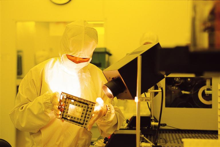
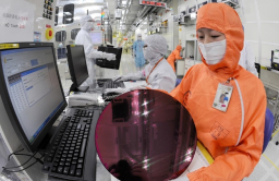
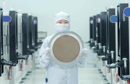
South Korea’s Samsung Electronics Co., the world’s largest memory chipmaker, will build a 40 billion yen ($281 million) advanced chip packaging research and development center in Japan amid improving ties between the neighboring countries.
Samsung will set up the research facility in Yokohama, southwest of Tokyo, to develop new chip packaging technology and deepen ties with Japanese makers of chipmaking equipment and materials, according to an announcement by the city of Yokohama and media reports.
Separately, Japan's industry ministry said it would offer Samsung subsidies worth up to 20 billion yen to support the revitalization of domestic chip manufacturing.
At the facility, Samsung will research back-end process technology in partnership with Japanese companies for artificial intelligence and 5G chips. Samsung expects the R&D center to strengthen its “leadership in chips.”
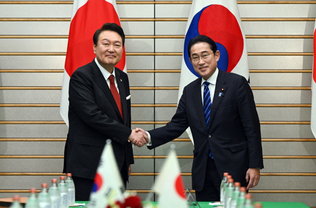
Samsung’s investment comes at a time of easing tensions between Seoul and Tokyo as the US encourages its two Asian allies to work together to counter China’s growing technological prowess.
At a summit meeting in Seoul on May 7, Korean President Yoon Suk Yeol and Japanese Prime Minister Fumio Kishida agreed to enhance the two countries’ chip alliance to improve the semiconductor supply chain.
TSMC, OTHER GLOBAL CHIPMAKERS RUSH TO TOKYO
Analysts said the Japanese government’s decision to pay for up to half of Samsung’s Yokohama R&D center symbolizes Tokyo’s determination to revive the island country’s once-mighty chip industry from decades of underinvestment and stagnant growth.
Amid heightened geopolitical tensions in Asia and technological rivalry between the US and China, Japan has been striving to bolster its chip supply chain by luring investment from firms abroad.
Global chip foundry leader Taiwan Semiconductor Manufacturing Co. (TSMC) is currently building its first Japanese chip plant in the western prefecture of Kumamoto as a joint venture with Sony. The facility 1 of the plant is scheduled for completion in February.
Semiconductor investments by foreign firms currently aided by the Japanese government include those by Micron Technology Inc. in Hiroshima Prefecture and Western Digital Corp. in Mie Prefecture.
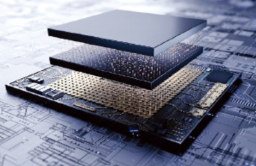
PACKAGING: NEXT BATTLE GROUND FOR CHIPMAKERS
Yokohama is home to another Samsung R&D institute.
In May, Samsung said it restructured its two R&D facilities – one in Yokohama and the other in Osaka – to launch an enlarged semiconductor research and development center in Japan, DSRJ.
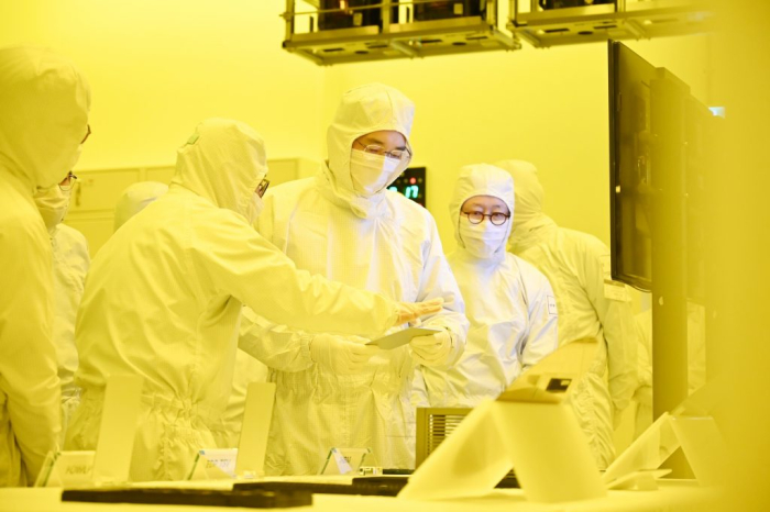
Samsung, a distant runner-up in foundry or contract chipmaking after TSMC, has been strengthening its research capabilities as demand for semiconductors grows across various industries, including AI, autonomous vehicles and 5G communications.
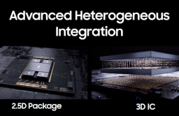
Last month, the Korean tech giant said it plans to unveil an advanced three-dimensional (3D) chip packaging technology next year to better compete with its archrival TSMC.
The technology, dubbed SAINT, or Samsung Advanced Interconnection Technology, will integrate memory and processors required of high-performance chips, including AI chips, in much smaller sizes.
Packaging, one of the final steps in semiconductor manufacturing, places chips in a protective case to prevent corrosion and provides an interface to combine and connect already made chips.
Packaging technology can enhance semiconductor performance without having to shrink the nanometer through ultra-fine processing, which is technologically challenging and requires more time.
According to consulting firm Yole Intelligence, the global advanced chip packaging market is forecast to grow from $44.3 billion in 2022 to $66 billion by 2027. Of that $66 billion, 3D packaging is expected to account for about a quarter, or $15 billion.
Write to Jeong-Soo Hwang at hjs@hankyung.com
In-Soo Nam edited this article.
More To Read
-
 Korean chipmakersSamsung to relocate packaging unit workplace to lure talent
Dec 14, 2023 (Gmt+09:00)
-
 Korean chipmakersSamsung to unveil 3D AI chip packaging tech SAINT to rival TSMC
Nov 12, 2023 (Gmt+09:00)
-
 Korean chipmakersSamsung narrows gap with TSMC in foundry market share
Sep 06, 2023 (Gmt+09:00)
-
 Korean chipmakersSamsung improves 4 nm foundry yields, on par with TSMC: analyst
Jul 11, 2023 (Gmt+09:00)
-
 Korean chipmakersSamsung on smooth track to 1.4 nm foundry tech to take on TSMC
Jun 28, 2023 (Gmt+09:00)