-
KOSPI 2812.05 +41.21 +1.49%
-
KOSDAQ 756.23 +6.02 +0.80%
-
KOSPI200 376.54 +6.64 +1.80%
-
USD/KRW 1373 3.00 -0.22%
Samsung to double HBM chip production to lead on-device AI chip era
Korean innovators at CES 2024
Samsung to double HBM chip production to lead on-device AI chip era
The world’s No. 1 memory maker has put its latest advanced AI chip series on display at CES 2024
By
Jan 12, 2024 (Gmt+09:00)
3
Min read
News+
Related Article
The Korea Economic Daily App


LAS VEGAS – Samsung Electronics Co., the world’s largest memory chipmaker, plans to more than double its high bandwidth memory (HBM) chip production volume as it aims to take the lead in the artificial intelligence chip segment.
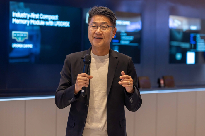
Han Jin-man, executive vice president responsible for Samsung's US semiconductor business, said on Thursday the company is pinning high hopes on high-capacity memory chips, including the HBM series, to lead the fast-growing AI chip segment.
“We will raise our HBM chip production volume by 2.5 times this year compared to last year’s output. The pace will continue with another twofold increase next year,” he told reporters during a media session at CES 2024.
“Memory chips will play the leading role in the AI era. Samsung will not be influenced by the industry’s ups and downs. We will steadily expand our investment in the growth sector,” he said.
Han is the highest-level Samsung executive to unveil the company’s HBM chip production plans for this year and next.
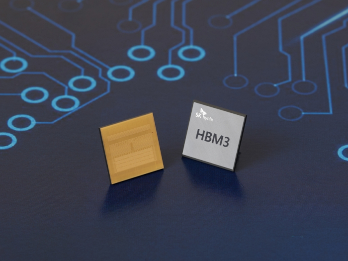
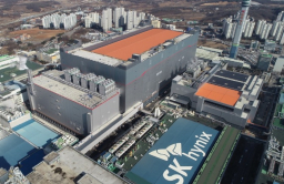
The Suwon, South Korea-based chipmaker has been striving to enhance its presence in the HBM segment, in which it is falling behind its crosstown rival SK Hynix Inc.
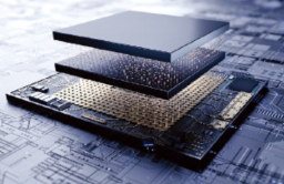
The HBM series of DRAM is the talk of the town these days as electronics makers are unveiling products equipped with on-device AI technology, which enables customized and personalized AI functions on smartphones and other smart gadgets.
HBM3, one of the most advanced such chips currently available, is said to have a capacity 12 times higher and a bandwidth 13 times higher than GDDR6, the latest DRAM product.
According to market tracker TrendForce, the global HBM market is forecast to grow to $8.9 billion by 2027 from an estimated $3.9 billion this year.
Last October, Samsung said it plans to unveil next-generation HBM4 chips in 2025 as part of its push to lead in the AI chip sector.
MEMORY-FOUNDRY TURNKEY SERVICE
Samsung said it aims to raise its HBM competitiveness by offering its clients a turnkey service, in which the company packages the graphic processing unit (GPU) made by Samsung Foundry and HBM chips into a single chipset.
“We’re positively considering producing next-generation HBM chips not at the memory process but at the foundry process to maximize business efficiency as we do both memory and foundry,” Han said at CES 2024.
Leading chipmakers such as foundry leader Taiwan Semiconductor Manufacturing Co. (TSMC) and Intel Corp. are fiercely competing for advanced packaging to enhance chip performance without having to shrink the nanometer through ultra-fine processing, which is technologically challenging and more time consuming.
In November, industry sources said Samsung plans to unveil an advanced three-dimensional (3D) chip packaging technology in 2024 to better compete with its rivals.
SAMSUNG’S NEW AI MEMORY CHIPS AT CES 2024
At this year’s electronics show, Samsung is showcasing several latest memory chips currently under development or already in supply to its clients.
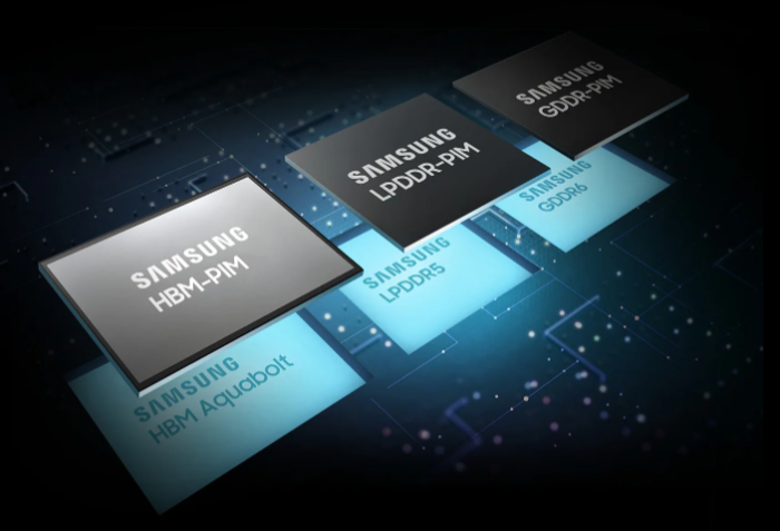
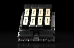
To meet growing demand from generative AI chip users, the company has put on display 12-nanometer 32-gigabyte double data rate 5 (DDR5) DRAM chips; Shinebolt, its HBM3E chip; and CMM-D, a computer express link (CXL) DRAM module.
For on-device AI functions, Samsung is showcasing LPDDR5X-PIM, an advanced DRAM chip that helps process data like a central processing unit (CPU).
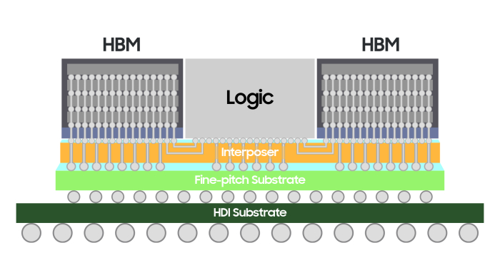
The company is also showing off its 2.5D packaging technology H-Cube and I-Cube series at CES.
“From 2025, chip demand will exceed supply. Barring the unexpected, client orders will rise significantly,” Han said.
Write to Jeong-Soo Hwang at hjs@hankyung.com
In-Soo Nam edited this article.
More To Read
-
 Tech, Media & TelecomSamsung ramps up on-device NPU chip R&D; LG Electronics joins race
Jan 07, 2024 (Gmt+09:00)
-
 Korean innovators at CES 2024Samsung dubs upcoming Galaxy S24 AI phone as on-device AI race rages on
Jan 04, 2024 (Gmt+09:00)
-
 Korean chipmakersSamsung to build $281 million chip packaging R&D center in Yokohama
Dec 22, 2023 (Gmt+09:00)
-
 Tech, Media & TelecomNew Samsung, LG laptops drive industry shift toward on-device AI
Dec 17, 2023 (Gmt+09:00)
-
 Korean chipmakersSamsung, SK pin hopes on HBM sales with Nvidia's new AI chip
Nov 14, 2023 (Gmt+09:00)
-
 Korean chipmakersSK Hynix bets on DRAM upturn with $7.6 bn spending; HBM in focus
Nov 09, 2023 (Gmt+09:00)
-
 Korean chipmakersSamsung to unveil 3D AI chip packaging tech SAINT to rival TSMC
Nov 12, 2023 (Gmt+09:00)
-
 Korean chipmakersSamsung set to supply HBM3 to Nvidia, develops 32 Gb DDR5 chip
Sep 01, 2023 (Gmt+09:00)