-
KOSPI 2577.27 -2.21 -0.09%
-
KOSDAQ 722.52 -7.07 -0.97%
-
KOSPI200 341.49 +0.02 +0.01%
-
USD/KRW 1396 -2.00 0.14%
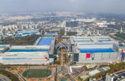
SK Hynix to produce HBM4 on 3 nm foundry process in 2025
Korean chipmakers
SK Hynix to produce HBM4 on 3 nm foundry process in 2025
It will apply the 12-nanometer foundry technology for general-use HBM4 and HBM4E
By
Dec 03, 2024 (Gmt+09:00)
2
Min read
News+
Related Article
The Korea Economic Daily App


SK Hynix Inc. will adopt the 3-nanometer process, the most advanced foundry technology available, to produce customized HBM4 chips in the second half of 2025, according to semiconductor industry sources on Tuesday.
The South Korean chipmaker had originally planned to manufacture the sixth-generation high-bandwidth memory (HBM4) tailor-made for customers on the 5 nm node. It is teaming up with foundry leader TSMC Co. to develop HBM4.
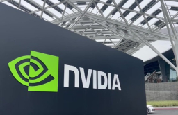
But it recently shifted to the 3 nm process for HBM4, which it is expected to ship to Nvidia Corp. in the second half of 2025, at the request of its key customers for more advanced memory.
SK Hynix is said to unveil a HBM4 prototype that is vertically stacked on a 3 nm base die as early as March, the sources told The Korea Economic Daily.
Nvidia's graphic processing unit (GPU) products are currently based on 4 nm HBM chips.
A base die is placed at the bottom of an HBM connected to a GPU and acts as its brain. An HBM stacked on a 3 nm base die is expected to enhance performance by 20-30% compared to the HBM4 with a 5 nm base die.
Its shift to a 3 nm foundry process comes as it goes all-in on US Big Tech such as Nvidia Corp., Google LLC and Microsoft Corp. to lessen its reliance on China amid Washington's clampdown on exports to China.

On Monday, Washington announced new semiconductor export controls against China. The latest package includes HBM chips.
SK Hynix commands about half of the world's HBM market and ships most of its HBM products to Nvidia, the largest AI chip buyer in the world.
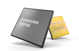
Producing HBM4 with a 3 nm base die will further widen its gap with Samsung Electronics Co., which plans to apply its 4 nm foundry process for sixth-generation HBM, or HBM4.
12 NM FOUNDRY FOR GENERAL-USE HBM4
For general-use HBM4 and HBM4E, SK Hynix will apply a 12 nm process technology in collaboration with TSMC.
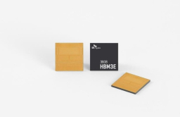
The world's No. 2 memory chipmaker manufactured HBM3E, or fifth-generation HBM, using its base dies. But for HBM4 chips, it has decided to adopt TSMC's technology.
TSMC mass-produces 3 nm memory chips embedded in Apple iPhones and MacBooks.
Nano refers to the width of the chip circuit line. The thinner the circuit linewidth, the more chips that can be mounted on the substrate or wafer.
SK Hynix is speeding up the development of HBM4 chips at Nvidia's request.
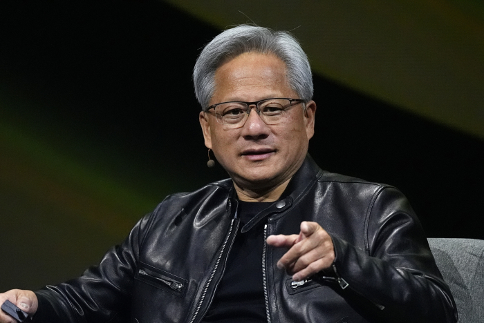
Nvidia’s CEO Jensen Huang recently asked SK Group Chairman Chey Tae-won to bring forward the supply of 12-layer HBM4 chips by six months from SK’s schedule of early 2026, Chey said in a keynote speech at the SK AI Summit 2024 last month.
Meanwhile, Tesla Inc. has called on Samsung and SK Hynix for samples of HBM4 prototypes for general use, South Korea’s semiconductor industry sources told The Korea Economic Daily last month.
After testing their prototypes, the world’s No. 1 electric vehicle maker is expected to choose one of the two companies as its HBM4 supplier.
Write to Chae-Yeon Kim and Jeong-Soo Hwang at Why29@hankyung.com
Yeonhee Kim edited this article.
More To Read
-
 Korean chipmakersTesla asks Samsung, SK Hynix to supply HBM4 chip samples
Nov 19, 2024 (Gmt+09:00)
-
 Korean chipmakersNvidia asks SK Hynix to bring forward HBM4 supply by 6 months
Nov 04, 2024 (Gmt+09:00)
-
Oct 31, 2024 (Gmt+09:00)
-
 Korean chipmakersSK Hynix chief says no delay in 12-layer HBM3E supply as demand soars
Oct 23, 2024 (Gmt+09:00)
-
 Korean chipmakersSK Hynix mass-produces 12-layer HBM3E for Q4 shipment
Sep 26, 2024 (Gmt+09:00)
-
 Korean chipmakersSamsung Electronics, TSMC tie up for HBM4 AI chip development
Sep 05, 2024 (Gmt+09:00)
-
Jul 31, 2024 (Gmt+09:00)
-
Jul 25, 2024 (Gmt+09:00)
-
 Korean chipmakersSamsung tipped to supply HBM3 to Nvidia for Chinese market
Jul 24, 2024 (Gmt+09:00)
-
 Korean chipmakersSamsung to mass-produce HBM4 on 4 nm foundry process
Jul 15, 2024 (Gmt+09:00)
-
 Korean chipmakersSK Hynix mulls HBM production in Japan, US
May 24, 2024 (Gmt+09:00)
-
 Korean chipmakersSamsung Elec to launch HBM4 in 2025 to win war in AI sector
Oct 10, 2023 (Gmt+09:00)